Photoshop or Gimp help
Discussion


Can anyone take me step by step on how to manipulate images of a printed circuit board.
I have a few broken brushless DC motors and they all suffer from a very common fault of a failed hall sensor.
The problem is the sensor is now obsolete and so is the package the chip uses, so I need to redesign the whole board, but to do so I need to make a schematic of the old one. Before the moderators jump on me, It's not piracy or copyright infringement to reverse engineer a printed circuit board, but to reverse engineer the software is.
I started working on the tutorials for Gimp and Photoshop but the learning curve is so step and I only want to use the software for this project alone.
Here's what I want.
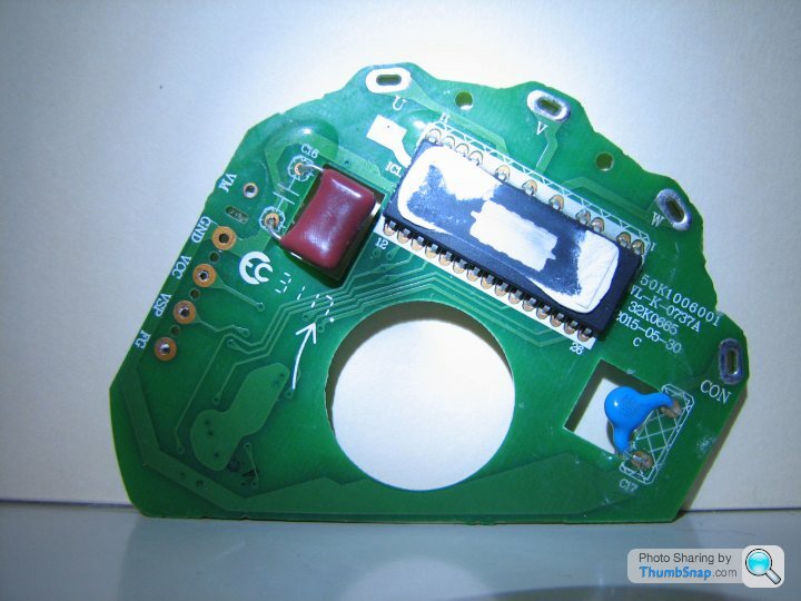
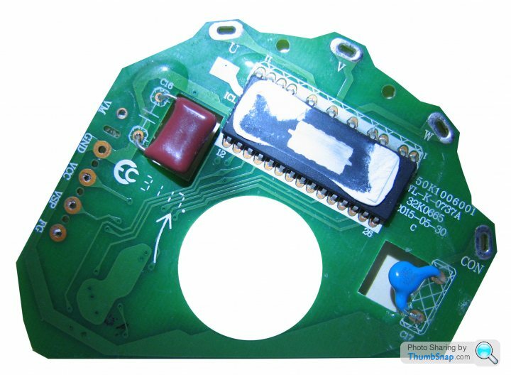
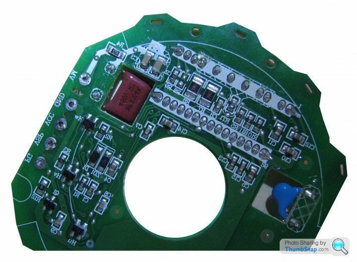
Top of the circuit board
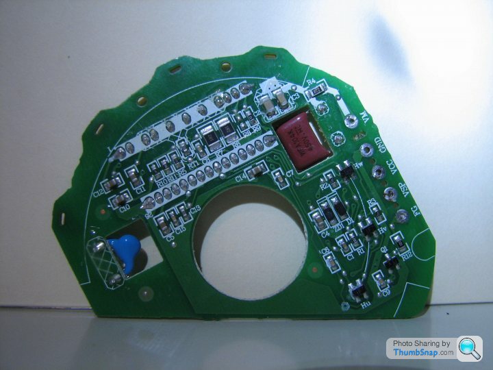
Bottom of the circuit board.
I want to flip one board and align both boards so that the outlines and mounting holes match, then draw the via's and traces for both top and bottom. With that I can work out what connects to what and recreate it with readily available components.
I've tried working with layers, but end up closing both programs and giving up (Very old dog and new tricks syndrome).
Anyone willing to help, please?
I have a few broken brushless DC motors and they all suffer from a very common fault of a failed hall sensor.
The problem is the sensor is now obsolete and so is the package the chip uses, so I need to redesign the whole board, but to do so I need to make a schematic of the old one. Before the moderators jump on me, It's not piracy or copyright infringement to reverse engineer a printed circuit board, but to reverse engineer the software is.
I started working on the tutorials for Gimp and Photoshop but the learning curve is so step and I only want to use the software for this project alone.
Here's what I want.
Top of the circuit board
Bottom of the circuit board.
I want to flip one board and align both boards so that the outlines and mounting holes match, then draw the via's and traces for both top and bottom. With that I can work out what connects to what and recreate it with readily available components.
I've tried working with layers, but end up closing both programs and giving up (Very old dog and new tricks syndrome).
Anyone willing to help, please?
My thoughts:
First, you need good source material. Set up the camera so it's perpendicular to the board, and have a nice flat light on the board. Take the first photo, turn the board over, take the second.
Open one image in PS and choose Image > Image rotation > Flip canvas horizontal. Select it with Ctrl-A then copy it with Ctrl-C.
Open the other image in PS. Ctrl-V will now past the first image over the second. You now have two layers. But as the top layer is 100% opacity, it will obscure the one underneath. In the Layers window, make sure the top image is selected, then slide its Opacity to 50%.
The circuit board should be exactly the same size in each image, so all you have to do now is use the Move tool until they're perfectly superimposed.
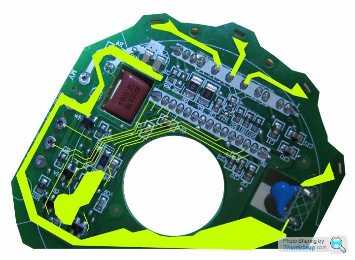
Does this help? (Yellow stuff is the tracks that can be seen on the top view).
Here's a 50% transparency version which might be useful:
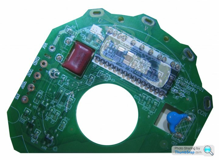
Also the top and bottom aligned so that you can give this a go. (Note that the text on the bottom is necessarily reversed):
Here's a 50% transparency version which might be useful:
Also the top and bottom aligned so that you can give this a go. (Note that the text on the bottom is necessarily reversed):
Edited by Turtle Shed on Tuesday 2nd August 11:15
Edited by Turtle Shed on Tuesday 2nd August 11:16
Turtle Shed said:
Does this help? (Yellow stuff is the tracks that can be seen on the top view).
Here's a 50% transparency version which might be useful:
Also the top and bottom aligned so that you can give this a go. (Note that the text on the bottom is necessarily reversed):
It's a wonderful help, but how did you do it?Here's a 50% transparency version which might be useful:
Also the top and bottom aligned so that you can give this a go. (Note that the text on the bottom is necessarily reversed):
Edited by Turtle Shed on Tuesday 2nd August 11:15
Edited by Turtle Shed on Tuesday 2nd August 11:16
I tried opening one of the images, rotating it, making a copy and pasting it which gave me 3 files, all with the same image but titles of background, layer 1 and layer 2.
I then open the other image and it simply opens in another 'page' that doesn't show the previous 3 images, so I have no idea how to get the two images into one 'page'.
Really struggling to understand this software.
NMNeil said:
I then open the other image and it simply opens in another 'page' that doesn't show the previous 3 images, so I have no idea how to get the two images into one 'page'.
Simpo Two said:
Select it with Ctrl-A then copy it with Ctrl-C. Open the other image in PS. Ctrl-V will now past the first image over the second.
You'll then have all the layers in one image. It's the difference between 'images' and 'layers in an image' that's foxing you. ^ What he said, but also note that you don't want to be rotating the second image, you need to mirror it (edit->transform->flip horizontal).
For completeness I did the following:
Open one image and duplicate it as a new layer.
Fill the initial layer with white
Open second image, drag it onto the first one (creating a third layer) and flip it horizontally
Give the top layer some transparency so that you can see how they align with each other
Then edit->transform->distort on that top layer and align it with the one below. It lines up pretty easily.
Draw a mask around the outside of one of the layers (with the tool that does straight lines, can't remember what it's called)
Invert the mask and hit delete to remove everything but the circuit board
With the mask still there select the other layer and hit delete again.
You now have two aligned layers, front and back, over a white background. If you fancy being clever you can use a circle mask for the middle of the circuit board and delete that on both layers to leave just the white background (No inversion this time, you've slected the bit you want to delete).
My final step was then to just create a new layer, and use the line tool to draw over the tracks with a nice bright colour. (Though I did also do a bit of masking stuff to colour over the bigger bits - mask around big bit, paint within it).
Not sure why you need anything as fancy as GIMP or photoshop.
Step 1, Download KiCAD and draw the schematic in eeschema.
Step 2. Place the PCB flat on a scanner alongside a rule and scan.
Step 3. Import to MS Paint, Make sure the outline of the PCB, the holes & the rule (for scale) are visible and save as a black and white bitmap.
Step 4. Import the bitmap into PCBNew and scale it. Create a board outline using the imported bitmap as a guide. Include the rule.
Step 5. Print the board outline at 1:1 scale and compare first to the rule (to check the scale is good) and then to the original PCB.
Step 6. Complete PCB layout as normal.
EDIT:
Oh, I get it. Sorry. You're looking to overlay the images and work out what connects to what.
I'm not sure why you'd think that this is any less of a copyright violation than reverse engineering software. Both are (probably copyrighted) intellectual property.
I'd start by scanning the PCB to get images that are same size and nice & square. Then use MS Paint to reduce each image to a single colour. Save the images as a 16 colour bitmap, trace the outline, vias and tracks and delete everything else. Working with 16 colours will make deleting the unwanted stuff nice and fast. When you save make sure everything you don't want is background coloured.
You can flip and rotate one image in MS Paint before saving.
Now import the two images into photoshop or GIMP as different layers. With the grunt work done in Paint it should be easy to overlay the two images and use transparency to get a PCB layout tool like view of the board.
Yeah, I do like MS Paint.It's simple and easy to use. It hasn't changed much since the 80's and it has the vast majority of the features you're looking for.
But frankly, for a simple PCB like that, I wouldn't bother with the image manipulation. I'd just pen and paper a schematic straight from the board.
Edited by BrokenSkunk on Wednesday 3rd August 12:41
BrokenSkunk said:
Not sure why you need anything as fancy as GIMP or photoshop.
Step 1, Download KiCAD and draw the schematic in eeschema.
Step 2. Place the PCB flat on a scanner alongside a rule and scan.
Step 3. Import to MS Paint, Make sure the outline of the PCB, the holes & the rule (for scale) are visible and save as a black and white bitmap.
Step 4. Import the bitmap into PCBNew and scale it. Create a board outline using the imported bitmap as a guide. Include the rule.
Step 5. Print the board outline at 1:1 scale and compare first to the rule (to check the scale is good) and then to the original PCB.
Step 6. Complete PCB layout as normal.
EDIT:
Oh, I get it. Sorry. You're looking to overlay the images and work out what connects to what.
I'm not sure why you'd think that this is any less of a copyright violation than reverse engineering software. Both are (probably copyrighted) intellectual property.
I'd start by scanning the PCB to get images that are same size and nice & square. Then use MS Paint to reduce each image to a single colour. Save the images as a 16 colour bitmap, trace the outline, vias and tracks and delete everything else. Working with 16 colours will make deleting the unwanted stuff nice and fast. When you save make sure everything you don't want is background coloured.
You can flip and rotate one image in MS Paint before saving.
Now import the two images into photoshop or GIMP as different layers. With the grunt work done in Paint it should be easy to overlay the two images and use transparency to get a PCB layout tool like view of the board.
Yeah, I do like MS Paint.It's simple and easy to use. It hasn't changed much since the 80's and it has the vast majority of the features you're looking for.
But frankly, for a simple PCB like that, I wouldn't bother with the image manipulation. I'd just pen and paper a schematic straight from the board.
Only a unique circuit can be copyrighted or patented, this is simply finding out where the copper traces connect. I'll be redesigning the complete circuit with off the shelf components none of which are patented or copyrighted. Imagine the chaos if the 555 chip schematic was copyrighted Step 1, Download KiCAD and draw the schematic in eeschema.
Step 2. Place the PCB flat on a scanner alongside a rule and scan.
Step 3. Import to MS Paint, Make sure the outline of the PCB, the holes & the rule (for scale) are visible and save as a black and white bitmap.
Step 4. Import the bitmap into PCBNew and scale it. Create a board outline using the imported bitmap as a guide. Include the rule.
Step 5. Print the board outline at 1:1 scale and compare first to the rule (to check the scale is good) and then to the original PCB.
Step 6. Complete PCB layout as normal.
EDIT:
Oh, I get it. Sorry. You're looking to overlay the images and work out what connects to what.
I'm not sure why you'd think that this is any less of a copyright violation than reverse engineering software. Both are (probably copyrighted) intellectual property.
I'd start by scanning the PCB to get images that are same size and nice & square. Then use MS Paint to reduce each image to a single colour. Save the images as a 16 colour bitmap, trace the outline, vias and tracks and delete everything else. Working with 16 colours will make deleting the unwanted stuff nice and fast. When you save make sure everything you don't want is background coloured.
You can flip and rotate one image in MS Paint before saving.
Now import the two images into photoshop or GIMP as different layers. With the grunt work done in Paint it should be easy to overlay the two images and use transparency to get a PCB layout tool like view of the board.
Yeah, I do like MS Paint.It's simple and easy to use. It hasn't changed much since the 80's and it has the vast majority of the features you're looking for.
But frankly, for a simple PCB like that, I wouldn't bother with the image manipulation. I'd just pen and paper a schematic straight from the board.
Edited by BrokenSkunk on Wednesday 3rd August 12:41

And I already have KiCad open, but had no idea about using MSPaint, so I'll give that a go, but my flatbed scanner blurs the image so I'll have to work with what I have. And I already started with pen paper and continuity tester, but it's so damn laborious.
Thanks for your help everyone.
You're assuming that the schematic follows the I.C. manufacturer's datasheet. If it doesn't it is IP belonging to the circuit designer.
If the schematic doesn't have any IP, why are you trying to reverse engineer it? Everything you need will be in the manufacturer's datasheet for the main IC.
To be clear, I think your assertion about there being no IP in the schematic is bunk. You can not possibly know that until you've reverse engineered it. I don't care that you're reverse engineering someone else's IP and I applaud the fact that you're having a go at redesigning an obsolete board. Which is why I'm trying to help.
I don't know how you're pen and pencilling the design, but don't try to draw a schem directly from the layout. I'd advise writing it as a netlist first.
e.g.,
Net 1: U1.1 to R1.2 to C12.1 to via to U2.1
Net 2: U1.2 to etc.
Where U1.1 is U1 pin 1.
Then go straight to eeschema from the netlist.
To get the PCB flat on your scanner & in focus you may need to remove larger components. You need to do that anyway to trace the tracks undernath them. Scanning is the way to go to get the outline right. You don't have to worry about camera lens distortion or getting the camera sensor parallel to the PCB.
Gassing Station | Photography & Video | Top of Page | What's New | My Stuff